
Cadence Teams Up with Google to Push AI-Driven Chip Design Further into the Cloud
Cadence is doubling down on AI-driven chip design, this time working closely with Google Cloud.
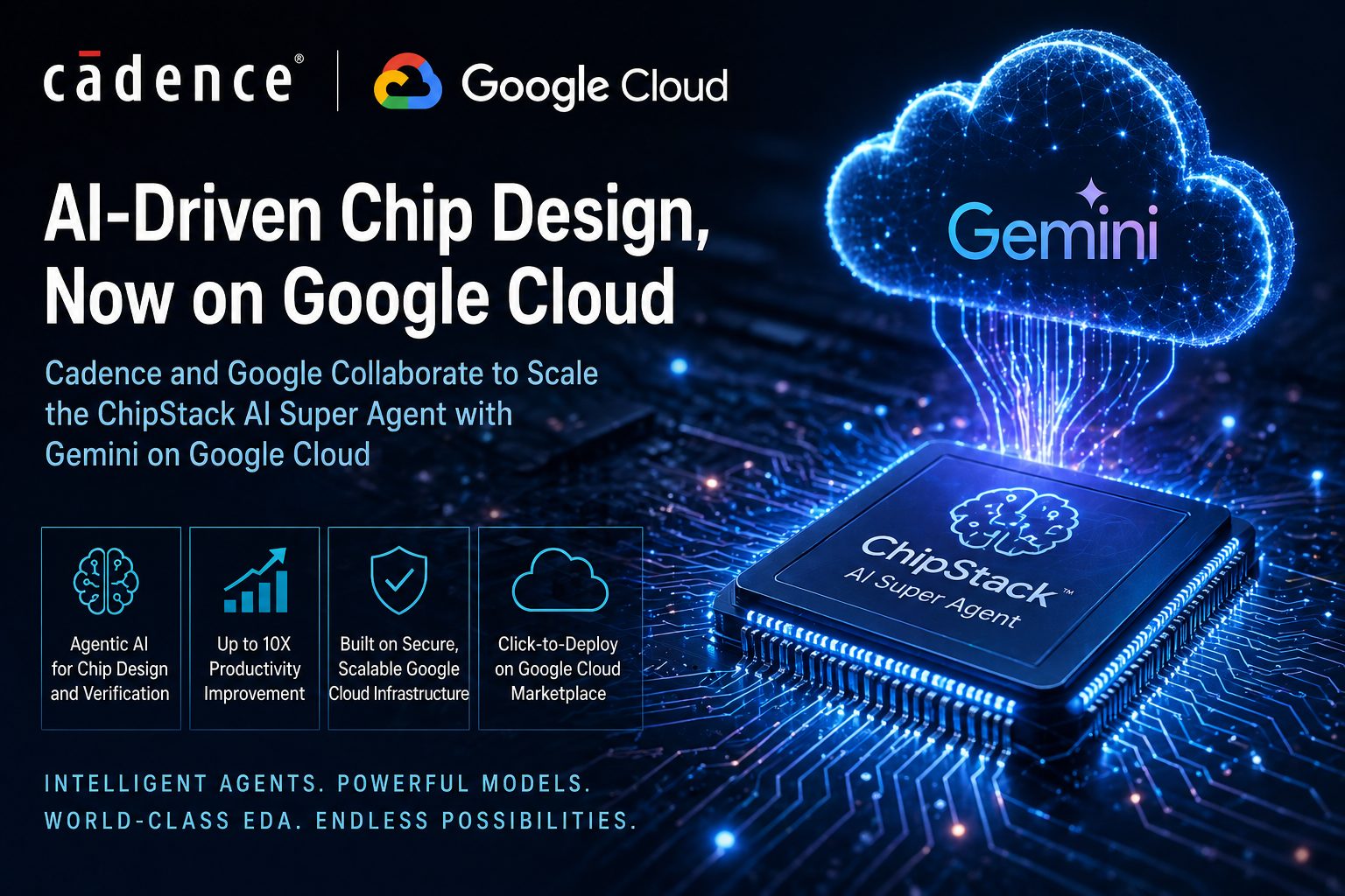
In its latest announcement, the company revealed a new collaboration that brings its ChipStack AI Super Agent together with Google’s Gemini models on Google Cloud. The objective is clear: make chip design faster, more scalable, and increasingly driven by intelligent automation instead of manual processes.
This is not just another AI integration story. It reflects a broader shift happening across the semiconductor industry, moving toward agent-driven design, where AI does more than assist engineers and starts taking on parts of the workflow itself.
Reducing the Manual Workload in Chip Design
Cadence’s ChipStack AI Super Agent is designed to work directly with its existing EDA tools, automating tasks that typically consume a large portion of engineering time. This includes areas such as verification planning, regression management, debugging, and parts of digital design.
Cadence reports that the platform is already delivering up to 10X improvements in productivity in certain workflows. That is a meaningful gain in an industry where development cycles are long and becoming increasingly complex.
By integrating Gemini, the system benefits from stronger reasoning capabilities and better context handling. In practical terms, this leads to more accurate outputs and more reliable assistance throughout the design process.
Addressing Trust and Accuracy
One of the main concerns when applying AI in engineering is whether the outputs can be trusted.
Cadence addresses this through what it calls its “Mental Model” approach. Instead of relying purely on raw AI-generated responses, the system uses Cadence’s own EDA knowledge and tools to guide the output. This ensures that results are not only syntactically correct, but also aligned with real-world engineering requirements.
In chip design, correctness is critical. Even small errors can have significant downstream impact, so this layer of control is essential.
Cloud as the Foundation
Google Cloud plays a key role in making this solution practical at scale.
Running large AI models like Gemini alongside intensive EDA workloads requires substantial computing power. By leveraging cloud infrastructure, Cadence allows teams to scale resources on demand without the need for heavy on-premise investments.
The availability of the ChipStack AI Super Agent on the Google Cloud Marketplace also simplifies deployment. Teams can adopt the solution quickly, without lengthy setup processes.
A Broader Industry Shift
This collaboration highlights a larger trend in the semiconductor space.
We are seeing:
- AI taking on more responsibility in design workflows
- Cloud platforms becoming the standard environment for development
- Traditional EDA tools evolving into AI-driven systems
Cadence is positioning itself at the center of this transition by combining its design expertise with advanced AI and cloud infrastructure.
Our Thoughts
What matters here is not just the technology, but the direction the industry is heading.
Chip design is reaching a level of complexity where manual workflows alone are no longer sufficient. The combination of AI agents and cloud computing is becoming a practical necessity rather than an experimental approach.
With NVIDIA focusing on simulation and digital twins, and Google bringing its AI capabilities into engineering workflows, Cadence is ensuring it remains competitive in a rapidly evolving space.
We are not at fully autonomous chip design yet. However, developments like this suggest that the industry is moving steadily in that direction, and likely faster than many expected.
Source: https://www.businesswire.com/news/home/20260415910313/en/Cadence-and-Google-Collaborate-to-Scale-AI-Driven-Chip-Design-with-ChipStack-AI-Super-Agent-on-Google-Cloud